Global Site
Displaying present location in the site.
Wavelength Conversion Technology Using Laser Sources with Silicon Photonics for All Photonics Network
Vol.17 No.1 September 2023 Special Issue on Open Network Technologies — Network Technologies and Advanced Solutions at the Heart of an Open and Green Society PDF
PDFInnovative optical networks are essential for the implementation and acceleration of advanced information and communication services such as autonomous driving and telemedicine. NEC is working to implement an All Photonics Network (APN) that enables transmissions with a low latency, low power consumption, and high capacity and that also makes full use of optical technology. The APN needs flexible wavelength conversion that is both compact in size and economical. NEC is therefore conducting R&D on ultracompact, dual-wavelength, tunable lasers as laser sources to be the key to wavelength conversion in APNs and using silicon photonics (SiP) that have a high-density integration and mass-production capability. This paper provides a report on the wavelength conversion technology and the technologies for the SiP and wavelength tunable laser sources that can realize a dual-wavelength, tunable laser.
1. Introduction
With the rapid development and spread of the Internet and smartphones, video streaming services as well as services based on cloud computing communications have become so familiar to the general public that information and communications technology (ICT) has become an indispensable part of our daily lives. As demands for further advancement of the Internet of Things (IoT), autonomous driving, and telemedicine increase, services capable of instantaneous transmission of larger amounts of information are required more than ever before.
Optical communication is one of the fundamental technologies supporting this ICT society. At present, the core networks connecting big cities in Japan through optical communications are putting large-capacity transmission systems in the terabit class into practical use. One of the key technologies supporting such large-capacity transmission is Dense Wavelength Division Multiplexing (DWDM), in which multiple wavelengths combine a variety of different signals onto a single optical fiber for transmission. In existing optical communication systems such as DWDM, the conversion between the optical and electrical signals is performed several times in the transmission path, and this becomes the dominant cause of delay. Delay poses a problem for implementation of services such as autonomous driving, which requires real-time performance. On the other hand, further expansion of transmission capacity requires an increase in energy consumption, which is a major problem. However, as miniaturization of semiconductors used in electrical processing has progressed to a level near the physical limit, the further reduction of the power consumption is said to be increasingly difficult.
To deal with such problems, NEC is striving to realize the All Photonics Networks (APN) that feature end-to-end (EtoE) communications using optical signals. APN are networks that minimize the conversion between optical and electrical signals; it can achieve an overwhelmingly low latency compared to conventional optical communication systems. APN can also drastically reduce network power consumption thanks to the low power requirement of optical signals even in large-capacity (high-speed) transmission. APN also provide end users with large-capacity services by assigning information to each of the DWDM wavelengths as described earlier.
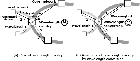
On the other hand, wavelengths are a finite resource, so technology for the efficient handling of wavelengths (or frequency bands) is necessary for the implementation of the ideal optical network needed for APNs. Fig. 1 shows a schematic diagram of an optical network. Although the optical signals from some local networks are concentrated in the core network, wavelength overlap must be avoided because signals of the same wavelength cannot be transmitted through a single optical link*1. For this purpose, flexible wavelength conversion is essential for the low-latency, power-saving, and high-capacity optical networks that everyone wants APNs to be. Also, because the EtoE optical path passes through several optical relays, some cases will differ in regard to the transmission distance, available wavelengths, and bandwidths before and after the optical relay devices. It is therefore thought that further improving the efficiency of wavelength resources by not only converting wavelengths but also flexibly changing to the optimal modulation format and optical signal bandwidth in accordance with the distance will accelerate the realization of APNs.
- *1Optical transmission path (optical fiber) interconnecting optical transmission devices.
2. NEC’s Concept of Wavelength Conversion Technology
As mentioned earlier, efficient wavelength/modulation format conversion technologies are important for the implementation of APN. In addition, because the installation space for optical transmission equipment is limited, a compact optical transmitter with the functions for wavelength/modulation format conversion is necessary.
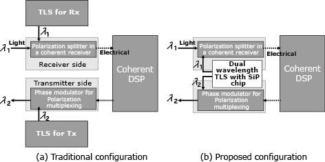
NEC was commissioned by the National Institute of Information and Communications Technology (NICT) to carry out R&D for an environmentally friendly and highly flexible, compact optical transmitter/receiver system that contains a compact, low-power optical transceiver which uses a high-speed, low-power digital signal processor (DSP) and silicon photonics (SiP) and that can switch wavelengths and modulation formats1). One of the components of the optical transmission system, the tunable laser source (TLS) is a key optical component for supporting large-capacity communications. Fig. 2 (a) shows a schematic diagram of a configuration in which wavelength/modulation format uses conventional TLS technology in a digital coherent system*2 for DWDM optical communications. TLS is required at both the transmitter and receiver sides. Conventional TLS uses a large number of components such as compound semiconductors, discrete optical components, and control circuit components, and this limits the miniaturization of the system. On the other hand, SiP technology has recently been gaining attention as way to create electronic and optical integrated circuits. SiP uses the manufacturing infrastructure of silicon CMOS (Complementary Metal Oxide Semiconductor) integrated circuits that possess excellent mass producibility and high-precision microfabrication. With the ability to form ultra-compact optical circuits, SiP technology enables the realization of a dual wavelength tunable laser source that integrates transmission and reception TLS in a single chip of the same size as conventional ones (Fig. 2 (b)) and thereby contributes to the miniaturization of optical transmission systems with the capability of wavelength/modulation format conversion.
- *2A transmission method that enables large-capacity transmission using amplitude, phase, and polarization of light by means of digital computations.
3. Toward Implementation of Dual Wavelength TLS
NEC has attained many achievements in the research of SiP and TLS technologies2)3)4). This section describes our efforts to realize a dual wavelength TLS being developed based on the knowledge acquired to date.
3.1 Principles and features of wavelength tuning
Silicon is used as the material for an optical waveguide in SiP to implement optical components with various functions in ultra compact optical circuits. This is because silicon has a very high refractive index (approximately 3.45), and the resulting tight optical confinement enables a layout of optical circuits with a bend radius of a few micrometers. Using a curved waveguide made of silicon, we confirmed a sufficiently low optical loss of less than 0.05 dB/turn at a bend radius of 10 μm across the entire C-band (1,525 to 1,565 nm), which was used as the communication wavelength band. NEC is making use of this advantage and designing an ultra compact SiP chip that can be used to freely control laser wavelength.
The schematic diagram of a TLS using the SiP chip under development is shown in Fig. 3. In this TLS, wavelength tunable operation is achieved with a double-micro ring resonator (D-MRR), which consists of two micro-ring resonators (MRRs) of different circumferences fabricated using SiP technology.
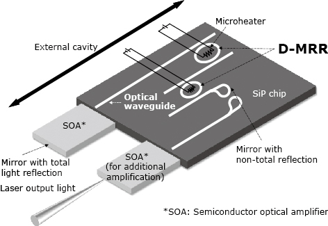
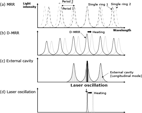
Images of transmission spectra are shown in Fig. 4. When a single MRR is used alone, a periodic transmission spectrum with a Lorentzian function appears, and the period of which determined by the circumference (Fig. 4 (a)). When using a D-MRR in which single MRRs are connected in series, the transmission spectrum is represented by the product of the MRR spectra. The maximum transmission factor is thus obtained at the wavelength where the transmission peaks of the two MRRs coincide with each other, and the D-MRR works as an optical wavelength filter (Fig. 4 (b)). A wavelength-tunable filter can be realized by adjusting the temperature of individual MRRs using a microheater placed in the proximity of each MRR to vary the wavelength at which the two transmission peaks coincide. In addition to the D-MRR, a mirror waveguide that is non-total reflection surface and has excellent loss characteristics is integrated into the SiP chip. The SiP chip is then combined with a semiconductor optical amplifier chip to form an external resonator (Fig. 3). By adjusting the cavity length so as to meet the required transmission wavelength of the D-MRR and the laser oscillation conditions of the external resonator (Fig. 4 (c)), laser oscillation at a single wavelength (Fig. 4 (d)) is achieved.
One advantage of the SiP-based TLS with an external resonator (SiP-TLS) is that the power consumption for tuning the laser oscillation wavelength is very low. This is because silicon has a very high thermo-optic coefficient (TOC) — which is about 20 times larger than conventional materials such as glass — and dictated by the rate of exponential growth (dn/dT)*3. NEC’s proprietary D-MRR design makes use of the high rate of exponential growth of silicon by optimizing the placements of microheaters to achieve wavelength tuning across the entire C-band from an ultra compact size of 150 x 100 µm2 and a low power consumption of 12 mW. NEC is also developing an MRR with an improved structure that is even more compact in size and an even lower power consumption.
Another advantage of the SiP-TLS is the capability of achieving a narrow, kilohertz linewidth required for expanding the capacity of digital coherent transmission4). To narrowing the laser linewidth, a long cavity of more than a few millimeters is required. SiP technology, however, is capable of layout with a bend radius of 10 µm, so this layout combined with the wavelength tuning mechanism of the D-MMR results in achieving long cavity on small chips.
- *3Variation in refractive index per 1°C temperature change.
3.2 Results of SiP-TLS prototyping
We prototyped a SiP-TLS with a single light source to verify the basic operations. Photo shows the prototype of an optical transmission module5). The SiP technology enabled us to achieve a very compact package. Further miniaturization can be expected by optimizing the structure.
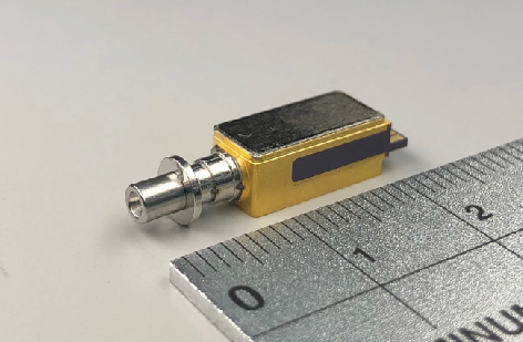
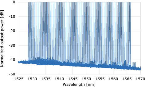
Fig. 5 shows a graph in which the laser oscillation spectra of SiP-TLS lasers at all 96 wavelengths used in DWDM are superimposed upon each other. The side mode suppression ratio (SMSR) that represents the monochromaticity of the laser is between 37 dB to 43 dB for every rate of laser oscillation, confirming favorable laser oscillation characteristics at all wavelengths.
At present, we are currently conducting research and development of a dual wavelength TLS that integrates two SiP-TLS functions on a single chip. We are also working on further reducing the power consumption, increasing the SMSR, and narrowing the linewidth. The dual TLS with its compact size and low power consumption enables NEC to contribute to the implementation of low-latency, power-saving, large-capacity APN.
- *4A package that incorporates laser elements, optical/electrical interfaces, etc.
4. Conclusion
This paper describes the wavelength conversion technology required for APN to support further development of the ICT society and the approach taken by NEC to develop the dual wavelength TLS that uses SiP technology for implementation. In the ideal network represented by the APN, the application of optical technology expands to terminals as well as transmissions over both short and long distances, so the importance and necessity of TLS are expected to increase further. For instance, a technology called co-packaged optics (CPO) in which the package of an electronic device such as a switch ASIC (Application Specific Integrated Circuit) is shared with an optical device has been attracting attention in recent years, and the CPO requires more than one laser source with a low power consumption and compact size. Dual wavelength TLS using SiP technology and multi-wavelength TLS with higher integration on a single chip are expected to be applicable to CPO. Meanwhile, SiP technology is not limited to laser light sources and is expected to be applied to the creation of more compact packages with several integrated functions, including optical modulators and photodiodes, as well as the development of new optoelectronic devices that combine optical functions and electronic circuits. NEC will continue to take on the challenge of realizing an environmentally friendly and more comfortable ICT society by developing the technologies for lasers and SiP, which have many possibilities to build on the optical technology that we have cultivated to date.
5. Acknowledgement
This paper includes results partly obtained through the “Research and development of compact and energy-efficient wavelength/format conversion technologies for beyond 5G ultra-high-speed and high-capacity networks (Key issue 04601)” commissioned by the National Institute of Information and Communications Technology of Japan.
References
- 1)
- 2)
- 3)
- 4)
- 5)
 National Institute of Information and Communications Technology: Beyond 5G R&D Promotion Project, Commissioned Research (Japanese)
Authors’ Profiles
MARUYAMA Ryo
Assistant Manager
Fiber Optic Devices Department
Assistant Manager
Fiber Optic Devices Department
KOBAYASHI Naoki
Assistant Manager
Fiber Optic Devices Department
Assistant Manager
Fiber Optic Devices Department
KURAHASHI Ryo
Fiber Optic Devices Department
Fiber Optic Devices Department
TAKAHASHI Morio
Senior Professional
Fiber Optic Devices Department
Senior Professional
Fiber Optic Devices Department