Global Site
Displaying present location in the site.
Black-Box Doherty Amplifier Design Method Without using Transistor Models
Vol.17 No.1 September 2023 Special Issue on Open Network Technologies — Network Technologies and Advanced Solutions at the Heart of an Open and Green Society PDF
PDFThis paper presents a newly developed realistic Doherty power amplifier (PA) design method with a black-box output combiner network. The method optimizes a realistic output network on the basis of ideal output network parameters with the black-box design by using the results of large-signal load-pull and S-parameter measurements without the need for transistor nonlinear models, which was required by the previous approach. The optimization considers main and auxiliary amplifier load modulations at back-off and peak output power levels. A 3.5 GHz 350 W Doherty PA with GaN-HEMT transistors is fabricated and measured to experimentally verify the method. The PA exhibits greater than 50% drain efficiency at 7 dB back-off and 57% peak drain efficiency at 6 dB back-off.
1. Introduction
The macro base stations in the Sub6 GHz range for the latest mobile communications, such as 4G, 5G or later, require high power amplifiers in order to achieve a large coverage area. The high power amplifiers are required to have high power efficiency over a wide power range in order to amplify orthogonal frequency division multiplexing signals, which have a high peak-to-average power ratio. A Doherty power amplifier (PA) can meet these requirements through transistor load impedance modulation1). A Doherty PA usually consists of two transistors. One is biased for Class AB, called the main amplifier, and the other is biased for Class C, called the auxiliary amplifier. Main and Auxiliary amplifier are combined with a quarter wave transformer. At maximum output power, the output matching network of main and auxiliary amplifier is tuned to the load impedance at the transistor drain, Ropt, which is the optimum load for maximum power2). At 6 dB back-off from maximum power, auxiliary amplifier is turned off and main amplifier is modulated to a 2 Ropt load. Thus, the conventional Doherty PA limits the load modulation from Ropt to 2 Ropt and does not necessarily achieve both the maximum output power and the maximum efficiency at the back-off level due to the limitation of the load modulation.
A black box design (BBD) method can ideally achieve both maximum output power and maximum efficiency at a desired back-off level by solving the output combiner network parameters based on four optimal load impedances for main and auxiliary amplifier3)4). BBD has theoretically obtained multiple solutions of the outputting network parameters. Since some of the plural solutions show significant efficiency drop, an optimal solution with high efficiency and high power at the same time is selected by using simulation. In addition, the realistic output network is obtained from the ideal output network calculated with the BBD method using simulation. Simulation usually requires the use of nonlinear transistor models from a vendor. Although the accurate nonlinear models are widely used in the industry, they are limited in the saturated power class of less than a few tens of watts. The nonlinear models of higher power devices are calculated by simple scaling. They are not accurate enough for 5G macro stations that require several hundred watts.
In this paper, we propose a newly developed realistic design method of the Doherty PA output network based on BBD. The method uses large-signal load-pull and small-signal S-parameter measurements using actual main and auxiliary amplifier instead of their transistor nonlinear models, which was necessary in the previous approach.
2. Doherty PA Design Method
A 3.5 GHz Doherty PA using an asymmetric twin-path GaN-HEMT device (Sumitomo Electric S35K29C18CM1P) is designed by the BBD method5). The device has 200W GaN-HEMT for main amplifier and 300W GaN-HEMT for auxiliary amplifier in one package. The quiescent current of main amplifier is 600 mA for class AB, and the gate bias of auxiliary amplifier is -5.0 V for class C. The drain bias of main and auxiliary amplifier is 50 V.
2.1 Calculating Theoretical Network Parameters with BBD
Fig. 1 shows the block diagram of a Doherty PA designed by the BBD method. Main and Auxiliary amplifier are connected to a lossy 2-port reciprocal network with ABCD network parameters T. The 2-port network T consists of two lossless 2-port reciprocal networks with ABCD network parameters Tm and Ta, and a resistive terminal load RL.
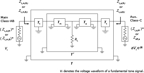
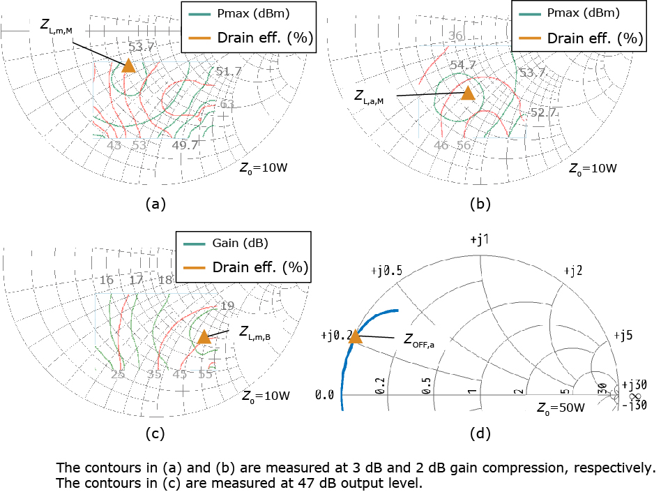
BBD uses the four target impedances ZL,m,M, ZL,m,B, ZL,a,M, and ZOFF,a to calculate the lossy reciprocal 2-port network T3). ZL,m,M and ZL,a,M are the load impedances for main and auxiliary amplifier, respectively, at maximum output power. ZL,m,B is the load impedance for main amplifier at back-off level. ZOFF,a is the output impedance of auxiliary amplifier when turned off. ZL,m,M and ZL,a,M are selected using the large-signal load-pull measurements shown in Fig. 2 (a) and (b) to achieve high maximum output power (Pmax) at the design frequency of 3.48 GHz. Fig. 2 (a) and (b) show the load-pull contours of main and auxiliary amplifier at constant gain compression of 3 dB and 2 dB, respectively. Main and Auxiliary amplifier are driven at the same input power level. ZL,m,B is selected by using the load-pull measurement of main amplifier at the constant output power of 47 dBm shown in Fig. 2 (c) to achieve high efficiency and gain at the back-off level. ZOFF,a is S22 at 3.48 GHz in the small-signal S-parameter measurement shown in Fig. 2 (d). The four impedances are set as follows,
ZL,m,M = 6.5 - j3.3 Ω (1)
ZL,m,B = 9.0 - j14.0 Ω (2)
ZL,a,M = 6.0 - j5.2 Ω (3)
ZOFF,a = 0.2 + j10.5 Ω (4)
The maximum output power of main amplifier at ZL,m,M is Pmax,MA = 53.7 dBm, and that of auxiliary amplifier at ZL,a,M is Pmax,AA = 55.0 dBm. Thus, the maximum Doherty PA output power is 57.4 dBm. At the back-off level of 47 dBm, the load-pull measurements of main amplifier at ZL,m,B show a drain efficiency of 45% and a gain of 19 dB, so the Doherty PA will have a drain efficiency of 45% and a gain of 16 dB.
BBD calculates the lossy reciprocal 2-port network T using (8), (27)-(30) in Reference [3]. T has many possible solutions depending on the phase offset between the output signals of main and auxiliary amplifier. The phase offset θ = -71° is chosen using (10) in Reference [3] so that the two 2-port networks of Tm and Ta are lossless.
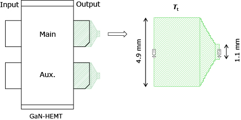
The output ports of the GaN-HEMT device have large widths due to the high output power, and the distance between the output ports of main and auxiliary amplifier is fixed because the device has two transistors in one package. Transmission lines having the same width as the device port restrict an actual microstrip layout for the output network calculated by BBD. Therefore, the port widths are transformed to 50 Ω line widths by using microstrip taper lines as shown in Fig. 3. The taper line of main amplifier has the same shape as that of auxiliary amplifier. The ABCD network parameters Tt of the taper line are estimated using Sonnet’s electromagnetic simulation engine and are extracted from the lossy reciprocal 2-port network T as follows,

where T’ is ABCD network parameters of the de-embedded lossy reciprocal 2-port network shown in Fig. 1. The transpose is denoted by (∙)T.
The two lossless reciprocal 2-port networks of Tm and Ta are calculated from the de-embedded 2-port network T’ using (23)-(29) in Reference [4]. Since the calculation of Tm and Ta is over-determined, Am = 0 is chosen to fix their solutions, where Am is the A -parameter of Tm. In addition, RL = 20 Ω is chosen to have the near maximum resistance that can realize the two 2-port networks, Tm and Ta, with two Π-networks. To realize the two Π-networks for Tm and Ta with capacitive stubs, the solutions for Tm and Ta calculated using the positive root of Dm, where Dm is the D -parameter of Tm, are chosen.
2.2 Design Method of a Realistic Schematic
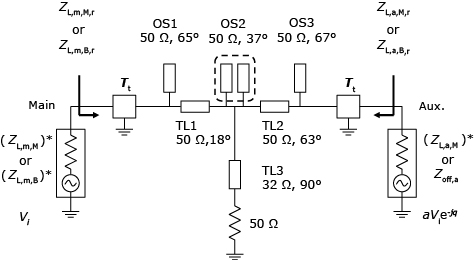
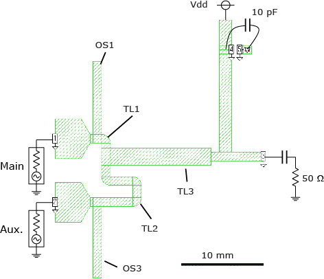
Fig. 4 shows a realistic schematic of the Doherty PA output network. The Π-network for Tm consists of the two open stubs, OS1 and OS2, and the transmission line TL1. The network for Ta consists of two open stubs, OS2 and OS3, and the transmission line TL2. The open stub OS2 merges the two open stubs of the two Π-networks for Tm and Ta. The transmission line TL3 is a λ/4 transformer to match the terminal load RL = 20 Ω to 50 Ω. The electrical lengths of OS1-OS3 and TL1-TL2 shown in Fig. 4 are the ideal values calculated from the ABCD parameters of Tm and Ta.
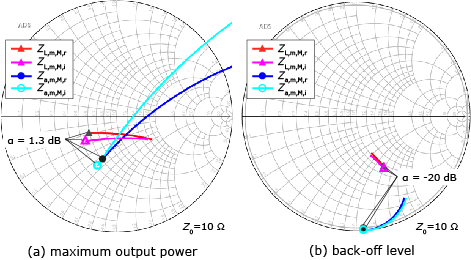
To design the microstrip layout of the output network, the electrical lengths of TL1-TL3 and OS1-OS3 are optimized using simulation. The simulation uses two power sources instead of the transistor nonlinear models of main and auxiliary amplifier. In the simulation at maximum output power, the source impedance of the power source for main amplifier is (ZL,m,M)*, and that for auxiliary amplifier is (ZL,a,M)*. The conjugate is denoted by (∙)*. At the back-off level, the source impedance of the power source for main amplifier is (ZL,m,B)*, and that for auxiliary amplifier is ZOFF,a. The signals generated by the power sources have a phase offset θ = -71° and an amplitude offset between main and auxiliary amplifier. The amplitude offset sweeps from (Pmax,AA/Pmax,MA) = 1.3 dB to -20 dB to simulate changing the output power of main and auxiliary amplifier. The maximum output power simulation estimates the two load impedances ZL,m,M,r for main amplifier and ZL,a,M,r for auxiliary amplifier, while the back-off level simulation estimates the two load impedances ZL,m,B,r for main amplifier and ZL,a,B,r for auxiliary amplifier. Similarly, simulation using the ideal schematic shown in Fig. 1 estimates the ideal load impedances of ZL,m,M,i, ZL,a,M,i, ZL,m,B,i, and ZL,a,B,i. The microstrip layout is optimized so that the realistic load impedances of ZL,m,M,r, ZL,a,M,r, ZL,m,B,r, and ZL,a,B,rZL,m,M,i match the ideal load impedances of ZL,m,M,i, ZL,a,M,i, ZL,m,B,i, and ZL,a,B,i, respectively.
Fig. 5 shows the optimized microstrip layout of the output network. The open stub OS2 is removed in the optimization process. Fig. 6 shows the comparison between the ideal load impedance and the realistic load impedance using the optimized microstrip output network. The realistic load impedance is almost the same as the ideal load impedance. The realistic load impedances ZL,m,M,r (α = 1.3 dB) and ZL,a,M,r (α = 1.3 dB), represented by the triangles in Fig. 6 (a), have a large influence on the maximum output power of the Doherty PA. The load impedance ZL,m,B,r (α = −20 dB), shown by the triangle in Fig. 6 (b), greatly affects the efficiency at the back-off stage.
3. Measurement Results
Photo shows a photograph of the fabricated Doherty PA. The printed circuit board uses a Rogers 4350B substrate that has a thickness of 0.5 mm.
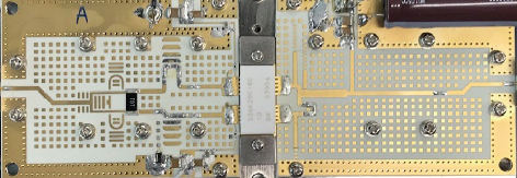
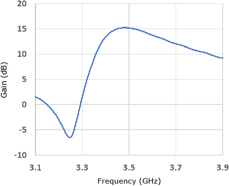
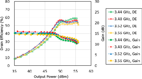
Fig. 7 shows the measured small signal gain. The peak small signal gain is 15.5 dB at the design frequency of 3.48 GHz. Fig. 8 shows the measured drain efficiency versus output power in pulsed continuous wave (CW) operation. The maximum power at 3.48 GHz is 55.5 dBm, which is slightly lower than the target power of 57.4 dBm. The decrease in maximum power is not caused by output network losses or phase mismatch between main and auxiliary amplifier because the fabricated PA has a sufficiently high drain efficiency of 56% at maximum power. The target maximum power of auxiliary amplifier, Pmax,AA, is 1.3 dB higher than that of main amplifier, Pmax,MA, while the gain at the target maximum power of auxiliary amplifier is about the same as that of main amplifier. To drive both main and auxiliary amplifier at maximum power simultaneously, the input level of auxiliary amplifier must be 1.3 dB higher than the input level of main amplifier. However, in this Doherty design, main and auxiliary amplifier are driven at the same input power level. Thus, the decrease in maximum power is mainly caused by the load impedances of main and auxiliary amplifier not being fully modulated to ZL,m,M and ZL,a,M, respectively, due to the low input power level of auxiliary amplifier. At the back-off level of 47 dBm, the fabricated PA has a measured drain efficiency of 44% and a gain of 15.5 dB, which agree well with the target efficiency of 45% and gain of 16 dB, respectively. This agreement between measured and target values indicates that the actual load impedances for main and auxiliary amplifier at the back-off level correspond to the target load impedances of ZL,m,B and ZOFF,a, respectively. The drain efficiency from 3.44 GHz to 3.56 GHz is greater than 50% at 6 dB back-off, and especially the drain efficiency from 3.48 GHz to 3.52 GHz is greater than 50% at 7 dB back-off. The peak drain efficiency at 3.48 GHz is 57% at 6 dB back-off.
4. Conclusion
This paper has demonstrated the Doherty PA BBD method using large-signal load-pull and S-parameter measurement results instead of transistor nonlinear models. Using this method, we have designed and fabricated the 3.5 GHz 350 W Doherty PA using an asymmetric twin-path GaN-HEMT device. The fabricated Doherty PA has achieved the high drain efficiency of more than 50% over a wide power range up to 7 dB back-off-level, and the measured drain efficiency matches the design target efficiency. The good agreement between the target and measured efficiencies, especially at the back-off level, indicates that the microstrip output network is correctly optimized from the ideal BBD output network by using the proposed method. The proposed method has great potential to properly design a high-power, high-efficiency Doherty PA using compound semiconductor transistors.
References
- 1)
- 2)
- 3)
- 4)M. Özen, K. Andersson and C. Fager: Symmetrical Doherty Power Amplifier With Extended Efficiency Range, IEEE Transactions on Microwave Theory and Techniques, Vol. 64, No. 4, pp.1273-1284, April 2016
- 5)
 W. H. Doherty: A New High Efficiency Power Amplifier for Modulated Waves, Proceedings of the Institute of Radio Engineers, Vol. 24, No. 9, pp.1163-1182, September 1936
Authors’ Profiles
OHGAMI Kazuya
Professional
Wireless Access Development Department
Professional
Wireless Access Development Department
TAWA Noriaki
Professional
Wireless Access Development Department
Professional
Wireless Access Development Department
de FALCO Paolo Enrico
Post Doctor
University of Colorado
Post Doctor
University of Colorado
BARTON Taylor
Professor
University of Colorado
Professor
University of Colorado
KANEKO Tomoya
Senior Professional
Wireless Access Development Department
Senior Professional
Wireless Access Development Department