Global Site
Displaying present location in the site.
Self-configuring Smart Surfaces
Vol.17 No.1 September 2023 Special Issue on Open Network Technologies — Network Technologies and Advanced Solutions at the Heart of an Open and Green Society PDF
PDFSmart Surfaces, also known as Reconfigurable Intelligent Surfaces (RISs), are expected to play a crucial role to achieve the key performance indicators (KPIs) for future 6G networks. The revolutionary advantage of this novel and emerging technology relies in the ability to control the propagation environment by changing the traditional communication paradigm that perceives the communication channel as an uncontrollable black box. We present our RIS design that can efficiently alter the reflection angle of the impinging wave. Additionally, we overcome the need for a fast and complex control channel by introducing a Self-configuring Smart Surface that can be easily and seamlessly installed without requiring modifications of the deployed mobile network.
1. Introduction
The ever-increasing need for network performance improvement has led to exploring new ways to push communication transmission efficiency that go beyond the classic communication paradigm. A revolutionary technology capable of providing control over the propagation environment has been recently introduced: Smart Surfaces, also known as Reconfigurable Intelligent Surfaces (RIS), raise the possibility of altering the way waves propagate in the environment in an intelligent, controllable, and flexible fashion, opening the possibility of optimizing it for unprecedented communication performance.
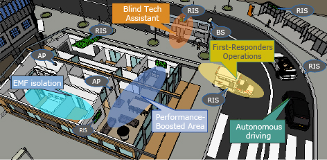
While this game-changing technology introduces a bulk of new business opportunities and advanced use-cases for the next generation of wireless networks (B5G/6G) as shown in Fig. 1, it involves a number of technical challenges to be addressed. The RIS paradigm transforms the propagation environment from an adversary to an optimizable communication ally actively contributing to improving performance, with the sole use of surfaces equipped with low-cost, and low-complexity electronics. The RIS technology, which typically refers to planar structures with almost passive electronic circuitry, i.e., without any power amplification, is envisioned to be jointly optimized with conventional wireless transceivers to significantly boost wireless communications in terms of coverage, spectral and energy efficiency.
Existing RIS prototypes are composed of discrete sets of electromagnetically excited elements with tunable responses and can be seen as either reflective or transmissive surfaces. Specifically, a reflective surface operates as an ElectroMagnetic (EM) mirror, where an incident wave is reflected towards the desired direction ― typically anomalous, i.e., this direction can diverge from geometrical optics ― with specific radiation and polarization characteristics. On the other hand, a transmissive RIS operates as a lens or a frequency selective surface, where the incident field is manipulated (by filtering, beam splitting, polarization change) and/or phase shifted, and re-radiated to control the refraction of impinging plane waves.
Although RISs have great potential to implement advanced EM wave manipulations, mainly simple functionalities, such as electronic beam-steering and multi-beam scattering, have been demonstrated in the literature. Only recently, RISs equipped with either minimal reception radio frequency chains or minimal power amplifiers have been introduced to enable sensing at the RIS side (which, apart from a standalone operation, can facilitate their network-wise orchestration) or reflection amplification (to confront the severe multiplicative pathloss), respectively. Within this context, we present our design of a self-configuring RIS that implements the hybrid reconfigurable intelligent surface (HRIS) technology by bringing built-in sensing capabilities to quasi-passive RISs.
2. RIS Design
We first describe our nearly-passive RIS design, externally controlled. The main purpose is to perform beamforming passively, i.e., refocus the energy received from impinging RF signals towards specified directions without active, i.e., energy-consuming RF components.
The designed board consists of a grid of 10 x 10 unit cells distributed in a 2D array, as depicted in Fig. 2. Unit cells are elements that can reflect RF signals with configurable phase shifts. Phase shifts are dynamically configured through a microcontroller unit (MCU), which can be programmed from an external controller. Conventional RIS designs are characterized by dedicated connections from the MCU to each unit cell. However, MCUs only support a limited number of such connections, which constrains the maximum number of cells and, consequently, the achievable beamforming gains. A more scalable approach can be obtained by connecting each cell with a pair of buses, denoted as column/row cell selection buses, that select the unit cell to be configured, and a phase configuration bus, which communicates the desired configuration index out of a discrete set. In this way, the complexity of the design is significantly reduced.
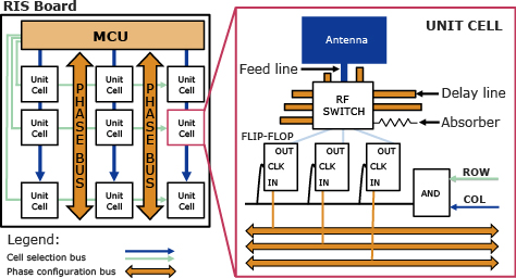
Flip-flop D: Each unit cell connects both column/row selection buses with an AND gate, as depicted in Fig. 2. When the MCU sets a high voltage state in a specific row and column, the MCU activates the configuration bus for such selected unit cell whereas all the remaining gates across the board will output a low voltage state (0V). Each cell also integrates a set of flip-flop D, which exploit the high state exiting the AND gate as a rising edge to update and send out the value stored in memory. Our RIS design implements 3-bit phase shifters, which enable high spatial resolution codebooks. Therefore, each cell uses three 1-bit phase configuration buses and three flip-flops.
RF-Switch: The latter are connected to configuration ports in an RF switch. An RF switch is a component that can redirect the RF signal received from an input port towards one output port, as indicated by the configuration ports. The input port is connected to a patch antenna, the ultimate responsible for interacting with the medium, through a feeding line. Each output port (except one) uses an open-ended delay line with a suitably designed length to reflect impinging signals with a specific time delay, shifting the signal phase.
Absorber: One output port of the RF switch is used to connect an absorber, an impedance-matching component that absorbs the energy of incoming signals instead of reflecting them back. This enables the absorption state, and it let us virtually optimize the reflective area of the RIS to meet system constraints. For instance, we can flexibly adapt to different time constraints when optimizing the RIS configuration. Alternatively, an energy harvester may be employed instead to reuse the dissipated energy to feed a low-consuming MCU, becoming self-sustainable boards.
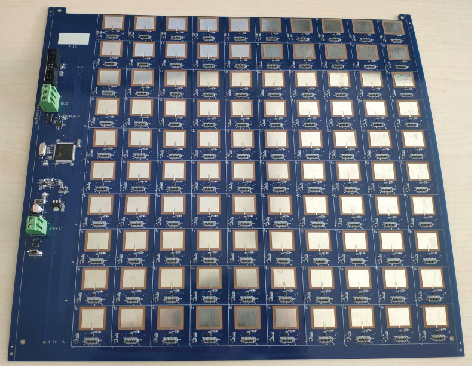
The suggested RIS design is modular: multiple boards can be coordinated through a common bus. The disposition of the unit cells across different boards has been carefully designed to have a separation of λ/2, where is the operating wavelength, as shown in Photo. Such modular boards let us increase/decrease the physical area of our structure without compromising the inter-cell distance.
3. Self-Configuring RIS
We go beyond the classical concept of nearly-passive Smart surface: we exploit the self-configuration concept that allows to remove the explicit control line from the above-described RIS design. This enables a new generation of RIS that can be flexibly installed without incurring in additional deployment complexity and cable clutter.
Our self-configuring RIS design takes into consideration an HRIS comprising an array of hybrid meta-atoms, which are able to simultaneously reflect and absorb (i.e., sense the power of) incident signals. In the considered architecture, each unit cell is coupled with a sampling waveguide that propagates the absorbed (i.e., sensed) power of the incident EM waves towards some downstream RF hardware for enabling digital signal processing.
To reduce the complexity and cost of the required hardware with respect to conventional HRIS, we propose HRIS that are not equipped with fully-fledged RF chains but only with an RF power detector. As shown in Fig. 3, the signals absorbed by each unit cell are summed together by means of RF combiners, which may be easily implemented as lumped components throughout the RIS RF circuit. The resulting signal is fed into an RF switch, which routes it to the above-mentioned power detector. The former converts the RF power into a measurable DC or a low-frequency signal, and is made by, e.g., a thermistor or a diode detector. The latter extracts energy from the EM fields in the form of DC voltage by means of a rectifier or a voltage multiplier that boosts the output DC by stacking multiple rectifiers, such as in the Cockcroft–Walton or Dickson configurations1). By leveraging on such components, we respectively enable HRIS self-configuration and energy self-sufficiency.

In the considered hardware architecture, the reflected and absorbed signals are subject to a phase shift applied by the unit cell. Each signal is fed to its corresponding phase shifter bank, which is optimized independently of the other, allowing us to simultaneously control the signal reflection and power absorption properties of the HRIS. We underline that independent phase shifter banks can be obtained at once by introducing one additional phase shifter at each meta-atom even starting from a dependent phase shifter banks design, though at the expense of higher circuit complexity.
4. Empirical Evaluation
Hereafter we show the empirical evaluation of our designed externally-controlled RIS prototype.
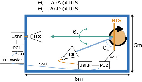
We characterized one of our 10 x 10 RIS board as described above, in 8 m x 5 m anechoic chamber. We mounted the board on a turntable controlled remotely from a master PC, which is also used to configure the beamforming parameters of the RIS. We use two software-defined radio devices attached to horn antennas with gain = 13.5 dBi to generate (“TX”) and receive (“RX”) a continuous stream of OFDM QPSK-modulated symbols with 5 MHz of bandwidth and numerology that meets 3GPP LTE requirements. The transmission power of TX is -30 dBm per subcarrier, and we sample the reference signal received power (RSRP) at RX.
As shown in Fig. 4, the distances RIS-TX (dRIX-TX) and RIS-RX (dRIX-RX)are 1.1 m and 6.3 m, respectively. Considering the size of the RIS approximately equal to 30 cm x 30 cm and its operating frequency (5.3 GHz), it is hard to guarantee that dRIX-TX is larger than the far-field threshold, which is ![]() , where = 0.43 m is the diagonal of the array. Nevertheless, our choice of dRIX-TX is larger than the reactive near-field threshold, which is
, where = 0.43 m is the diagonal of the array. Nevertheless, our choice of dRIX-TX is larger than the reactive near-field threshold, which is ![]() , and sufficient for our purposes. The rotation of the table determines the azimuth angle, and the location of TX determines θt. Conversely, the elevation angles of dRIX-TX and dRIX-RX are fixed to φt = 33° and φr = -3°, respectively.
, and sufficient for our purposes. The rotation of the table determines the azimuth angle, and the location of TX determines θt. Conversely, the elevation angles of dRIX-TX and dRIX-RX are fixed to φt = 33° and φr = -3°, respectively.
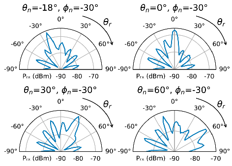
We empirically validated our RIS prototype. Fig. 5 depicts some representative RIS configurations. It shows that the main beam points towards the intended directions. We note, however, that the gain of the main lobe is penalized when we use large steering angles. Overall, the power received in the intended direction ranges between -74 dBm (for large steering angles) and -64 dBm (for smaller angles), which give us remarkable beamforming gains between -17 dB and -27 dB over the noise floor. Using the radar range equation2), the peak Radar Cross Section (RCS) can be calculated as ![]() .
.
References
- 1)
- 2)Constantine A Balanis: Antenna theory: analysis and design, John wiley & sons, 2016
 L. Tran et al.: RF power harvesting: a review on designing methodologies and applications, Micro and Nano Systems Letters 5, Article number: 14, 2017
Authors’ Profiles
SCIANCALEPORE Vincenzo
Principal Research Scientist
6G Networks
NEC Laboratories Europe
Principal Research Scientist
6G Networks
NEC Laboratories Europe
ROSSANESE Marco
Research Associate
6G Networks
NEC Laboratories Europe
Research Associate
6G Networks
NEC Laboratories Europe
MURSIA Placido
Research Scientist
6G Networks
NEC Laboratories Europe
Research Scientist
6G Networks
NEC Laboratories Europe
DEVOTI Francesco
Senior Research Scientist
Systems and Machine Learning
NEC Laboratories Europe
Senior Research Scientist
Systems and Machine Learning
NEC Laboratories Europe
GARCIA-SAAVEDRA Andres
Principal Research Scientist
6G Networks
NEC Laboratories Europe
Principal Research Scientist
6G Networks
NEC Laboratories Europe
COSTA PEREZ Xavier
Manager
6G Networks
NEC Laboratories Europe
Manager
6G Networks
NEC Laboratories Europe