Global Site
Displaying present location in the site.
Development of Nano-carbon Materials for IoT Device Applications
NEC Corporation is the originator of the carbon nanotubes (CNTs) and carbon nanohorn aggregates (CNHs) of representative nanomaterials. CNTs show either metallic or semiconducting properties that depend on differences in the arrangement of carbon hexagons. The thin film transistors that utilize the semiconducting CNTs are expected to extend application in the electronics domain. The CNHs have a high specific surface area and feature high dispersion and they are expected to be applicable to energy devices such as capacitor and fuel cell electrodes. More recently, NEC Corporation has discovered the carbon nano-brush (CNB), which is attracting much interest because it possesses the excellent properties both of the CNTs and the CNHs. This paper introduces NEC Corporation's current nanocarbon materials developments.
1. Introduction
The carbon nanotubes (CNTs)1) and carbon nanohorn aggregates (CNHs)2) are nanocarbon materials discovered by Sumio Iijima, Senior Research Fellow at NEC Corporation. They are expected to function as innovative materials that are capable of improving the characteristics of sensors, energy devices and composite materials. NEC is conducting wide-ranging R&D on these nanocarbon materials, from their fabrication to their device applications. A new nanocarbon material called the carbon nano-brush (CNB, fibrous carbon nanohorn aggregate) has recently been discovered3) and its excellent properties are expected to be applicable in various functions.
2. Carbon Nanotube
2.1 Features of the carbon nanotube
The carbon nanotube (CNT) is a carbon material discovered in 1991 by Iijima, as described above. It has a cylindrical structure with a diameter of 1 nm (one billionth of a meter) and it is composed of hexagonal carbon networks as is graphite (Fig. 1 (a) and (b)). The single-walled CNT is expected to have various applications due to its features that include a special shape, toughness, high electrical conductivity and high thermal conductance. Another feature of this material is that it presents a semiconducting or metallic properties that depends on the arrangement of the carbon hexagons (chirality). The ratio of the semiconducting and metallic species is respectively 2:1 in general.
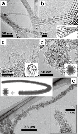
(The inserted diagrams are of relevant models).
2.2 The Metallic/semiconducting separation technology of CNT and its applications in sensors
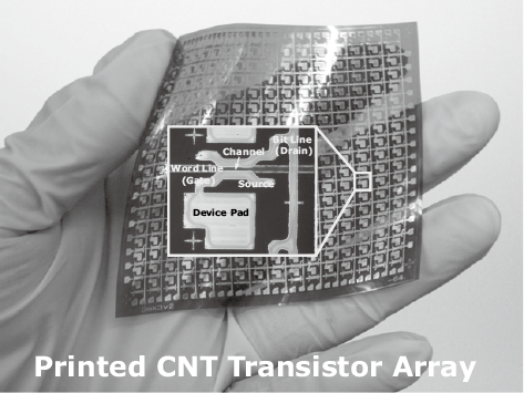
Semiconducting single-walled CNT is attracting attention as a material that uses printing technology for procedures in printed electronics that fabricate electronic products, such as circuitries. Using the semiconducting single-walled CNT with high electron mobility and chemical stability as a transistor channel material makes it possible to fabricate sensor devices with large areas, high flexibility, low prices, high operation speeds and high chemical stability. These properties are essential for IoT (Internet of Things) applications. NEC has developed the electric-field induced layer formation (ELF) method capable of extracting semiconducting single-walled CNT with the high purity of 99% or more4). This method achieves stable separation of the semiconducting and metallic single-walled CNTs by dispersing the single-walled CNTs using nonionic surfactant and moving them respectively to the cathodes and anodes by means of carrier-free electrophoresis (Fig. 2). The printed transistor array (Fig. 4) is fabricated with a highly functional ink made of the semiconducting single-walled CNTs based on this technology (Fig. 3). The process presents a tenfold or more times higher mobility than that with amorphous silicon. Here, the 256 devices are evenly separated into on and off states and a 6-digit on/off ratio is achieved5). The operation of a pressure sensor device using this transistor array has been tested and a multipoint dynamic pressure distribution was detected successfully. In the future, the material is expected to be utilized in IoT applications such as for the commodity management of convenience stores and warehouses.
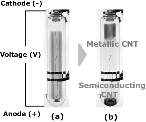
((a) Before separation, (b) After separation).
3. Carbon Nanohorn Aggregates
3.1 Features of the carbon nanohorn aggregates
The carbon nanohorn aggregates (CNHs) are nanocarbons discovered in 1998 by Iijima as described above. Each carbon nanohorn (CNH) has a cylindrical structure made of a single graphene sheet (Fig. 1 (c)) that resembles the structure of the single-walled CNT. The roll-shaped structure has a tip with a conical angle of about 19°, a diameter with a closed structure containing 5-membered rings of 2.5 nm and a length of 40 to 50 nm (Fig. 1 (c)). CNH does not exist singly but some thousands gather in a radial shape to form a spherical aggregate with a diameter of about 100 nm (Fig. 1 (d)). The internal nanospace of the CNH can be used by treating the tip and defect area with oxidation (hole-opening treatment). NEC has already developed a technology for the mass-production of high-quality CNHs at a low cost and is currently marketing samples and developing various applications.
3.2 Mass-Production Technology of Carbon Nanohorn Aggregates and Its Applications
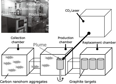
The CNHs can be fabricated by irradiating CO2 lasers onto a graphite target not containing a metal catalyst, in an Ar gas atmosphere at room temperatures. Fig. 5 shows a schematic depiction of the CNHs mass-production system6). This system is composed of three chambers: the graphite target storage chamber (Replacement chamber), the laser irradiation chamber (Production chamber) and the CNHs collection chamber. The Ar gas enters the laser irradiation chamber from below and is exhausted from the top of the collection chamber. After the COs laser irradiation, the graphite target in the storage chamber is automatically replaced. To reduce the number of graphite target replacements and the time taken to do this, large graphic targets with a diameter of 100 mm and a height of 500 mm are used. The CO2 laser is output at 3.5 kW in the continuous oscillation mode, and the target is rotated spirally at 2 rpm during the output in order to prepare CNHs continuously. The produced CNHs are carried by an Ar flow through the pipe and dropped when they reach the collection chamber. They are then caught in the collector vessel and are collected by closing the gate. Using this system, NEC has succeeded in the continuous production of CNHs at 100 g/h, 1 kg/day.
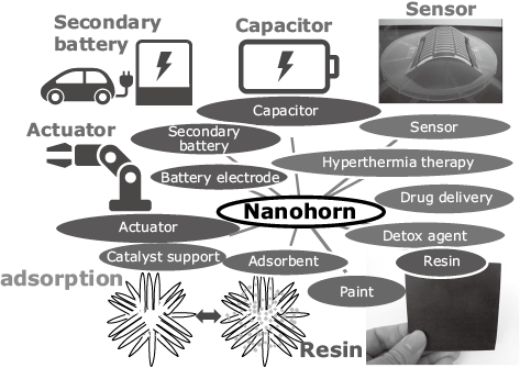
As the CNHs have a relatively large specific surface area of 400 m²/g and high electrical conductivity, it is expected that they will be applicable as catalytic support for fuel cells or as the conducting material of lithium ion batteries. The nanospace inside the sheath of the CNHs can be used by forming holes on each CNH by oxidation, and the specific surface area becomes as large as 1,420 m²/g or more in this case7). Because of this feature, R&D into the utilization of the nanospace is being actively conducted and applications such as for gas absorbents, electrodes of electric double-layer capacitors (EDLC), and drug delivery systems (DDS) are anticipated (Fig. 6).
4. Carbon Nano-brush
4.1 Features and expected applications of the carbon nano-brush
The carbon nano-brush (CNB, fibrous carbon nanohorn aggregate) was discovered by Ryota Yuge, Principal Researcher at NEC Corporation, in 2015 (Fig. 1 (e))3). The CNB structure resembles a test tube brush or pipe cleaner; in which individual single-walled carbon nanohorns gather radially and connect fibrously. The CNB can be fabricated by the laser ablation of a carbon target containing iron. CNB and CNHs are produced together by this process. As the fabrication method is almost identical to the already established method for the CNHs except for the target used, it is regarded that mass-production will be achieved relatively easily. CNBs feature not only the high dispersion and high adsorption as for the traditional spherical CNHs, but also exhibit high conductivity and is therefore expected to have wide applications in the future. The CNB is highly dispersive like the CNHs. When a mixture of CNB and CNHs in ethanol is dispersed with ultrasonic dispersion and the dynamic light scattering of the solution is measured, particle size distributions are detected in the ranges of 70-300 nm and 1-10 µm. The size distribution at the micrometric order seems to belong to the CNB. Like the CNHs, the specific surface area of the CNB is increased greatly at around 1,600 m²/g, by oxidation. When comparing the electrical resistivity of the thin films fabricated on SiO2 substrate by using CNB/CNHs mixture and CNHs alone, the CNB/CNHs mixture was 1/10th of that for the CNHs. This result showed that the CNB has an electro-conductive path in the one-dimensional direction. Therefore, it can be concluded that the CNB is a highly practical material featuring high electrical conductivity, high dispersion and a large specific surface area.
4.2 Applications of Carbon Nano-brush
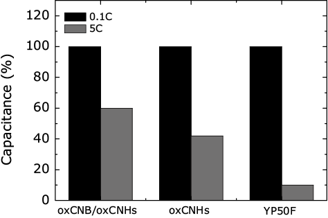
Since the EDLC needs to store high charges and input and output them rapidly, the electrode material should fulfill requirements such as high specific surface area, high electrical conductivity, and high dispersion. As the CNB meets these requirements, it is optimum for use with the EDLC. Fig. 7 shows the capacity retention rates of the EDLC prepared by using CNB/CNHs mixture after oxidation (oxCNB/oxCNHs), CNHs after oxidation (oxCNHs), and commercially available YP50F (activated carbon) as the electrode material. The specific surface areas and capacitances of the oxCNB/oxCNHs, oxCNHs, and YP50F are almost identical but that the use of oxCNB/oxCNHs succeeds in improving the output characteristics (fast discharge) by more than 6 times that of the commercially available YP50F.
5. Conclusion
The present paper introduces the development of CNT, CNHs, and CNB materials by NEC Corporation. The separation technology of an excellent metallic- and semiconducting-CNT, called the electric field induced layer formation method, has been developed that will soon be of practical use. As the transistors fabricated with this technology will feature high performance and stability, its applications in the electronics domain are regarded as likely to be accelerated. On the other hand, as the mass-production technology of the CNHs is already established, manufacturers other than NEC, such as the reagent manufacturers, have started to market high-quality CNHs and their developments aimed at commercialization are advancing impressively. Finally, with regard to the CNB, active R&D has been conducted since its discovery in 2015, including that for the evaluation of physical properties and the possibilities of applications. As described above, NEC has been creating and achieving practical applications for the new nanocarbon material technologies, one after the other. In the future, the corporation will apply these innovative nanocarbon materials to more of its products.
Reference
- 1)
- 2) Sumio Iijima et al.:Nano-aggregates of single-walled graphitic carbon nano-horns, Chemical Physics Letters) Volume 309, Issue 3, pp.165-170, August 1999
- 3)
- 4)
- 5) Hideaki Numata et al. :Adhesion property of carbon nanotube micelles for high-quality printed transistors, Proc. Int. Conf. 2016 IEEE 16th International Conference on Nanotechnology, pp.849-852, August 2016
- 6)
- 7)

Authors' Profiles
YUGE Ryota
Principal Researcher
System Platform Research Laboratories
Principal Researcher
System Platform Research Laboratories
IHARA Kazuki
Assistant Manager
Data Science Research Laboratories
Assistant Manager
Data Science Research Laboratories
NUMATA Hideaki
Principal Researcher
System Platform Research Laboratories
Principal Researcher
System Platform Research Laboratories
NIHEY Fumiyuki
Principal Researcher
Data Science Research Laboratories
Principal Researcher
Data Science Research Laboratories