
Global Site
Breadcrumb navigation
NEC's “Electron Microscope Used to Discover Carbon Nanotubes” Certified as a Japan Physical Heritage Instrument
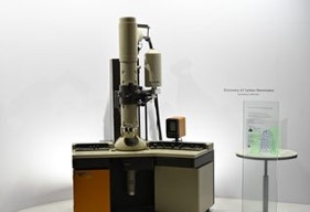
Tokyo, September 28, 2026 - NEC Corporation’s (NEC; TSE: 6701) “Electron Microscope Used to Discover Carbon Nanotubes” has been named one of the inaugural recipients of the “Japan Physical Heritage” (*1) certification, established by the Physical Society of Japan (JPS).
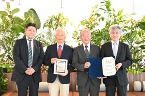
(From left) Ryota Yuge, Senior Principal Researcher, NEC; Sumio Iijima, Senior Research Fellow, NEC; Seiji Miyashita, President, Physical Society of Japan; Akio Yamada, Executive Officer, Corporate EVP & CAIO, NEC
The high-resolution transmission electron microscope "Topcon EM-002B," was used by Sumio Iijima, Senior Research Fellow at NEC, to discover multi-walled carbon nanotubes in 1991 (*2) and single-walled carbon nanotubes in 1993 (*3), the first discoveries of their kind in the world. Carbon nanotubes (CNTs) are now widely utilized for purposes ranging from fundamental physics to industrial applications, and this microscope is certified as the starting point of that development.
This electron microscope enabled imaging of fine structures in materials and crystal structure analysis via electron diffraction and was crucial for elucidating the atomic arrangement and concentric cylindrical structure of carbon nanotubes. These discoveries greatly advanced research in nanoscale physics, nanoelectronics, and materials science globally.
The “Japan Physical Heritage” program was established by the Physical Society of Japan to conserve and pass on historical materials related to physics, promote awareness of physics’ contributions to society, and foster pride in the achievements of pioneers.
This recognition has significant meaning in preserving awareness of the experimental apparatus that produced such a groundbreaking research achievement—the discovery of carbon nanotubes—for future generations, and in communicating NEC’s long-standing strengths in research and development.
Going forward, NEC will continue to carefully preserve historical research achievements and the technologies and expertise that supported them, while striving to create new social value through R&D in advanced technologies such as AI.
***
Notes:
- (*1)Physical Society of Japan, Japan Physical Heritage
 https://heritage.jps.or.jp/en/
- (*2)"Helical microtubules of graphitic carbon," Sumio Iijima, Nature, 354, 56-58 (1991)
- (*3)"Single-shell carbon nanotubes of 1-nm diameter," Sumio Iijima and Toshinari Ichihashi, Nature, 363, 603-605 (1993).
The Physical Society of Japan Official website:
About NEC
The NEC Group leverages technology to create social value and promote a more sustainable world where everyone has the chance to reach their full potential. NEC Corporation was established in 1899. Today, the NEC Group’s approximately 110,000 employees utilize world-leading AI, security, and communications technologies to solve the most pressing needs of customers and society.
For more information, please visit https://www.nec.com, and follow us on LinkedIn and YouTube.

NEC is a registered trademark of NEC Corporation. All Rights Reserved. Other product or service marks mentioned herein are the trademarks of their respective owners. © NEC Corporation.