NEC testing highly radiation-hardened semiconductor chip in space
- Mounted on JAXA satellite to assess operation reliability -
Tokyo, January 18, 2019 - NEC Corporation (NEC; TSE: 6701) today announced that it has developed a highly radiation-hardened (radiation-resistant) semiconductor chip, the "NanoBridge-FPGA (NB-FPGA)*1," and that it aims to demonstrate the operational reliability of the chip in space. This chip was developed utilizing results from a project*2 coordinated by the New Energy and Industrial Technology Development Organization (NEDO).
On January 18, 2019, Japan Aerospace Exploration Agency (JAXA) launched the "RAPid Innovative payload demonstration Satelite-1 (RAPIS-1)," equipped with NEC's newly developed NB-FPGA, on the fourth Epsilon Launch Vehicle (Epsilon-4) under JAXA's innovative satellite technology demonstration program. JAXA and NEC are now starting joint collection and evaluation of basic data on the NB-FPGA, including error rate measurement, in a space environment where radiation is very high. In addition, the reliable operation of image data compression is also being verified.
"Based on the results of this demonstration, we aim to promote the full operationalization of the NB-FPGA. We will also continue to expand its application into fields that include a wide range of vehicles, medical devices and satellite equipment, as we aim to advance the sophistication of IoT equipment and energy conservation," said Tadahiko Sugibayashi, Senior Manager, System Platform Research Laboratories, NEC Corporation.
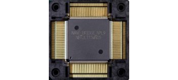 Fig. 1: NanoBridge-FPGA
(28 mm ×28 mm)
 ©JAXA
©JAXA
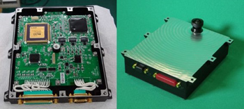
Fig. 2: Camera module equipped with NanoBridge-FPGA
(Developed by JAXA)
1. Outline
Against the background of an increasing need for the high-speed processing of big data, such as images and the acceleration of IoT, the adoption of FPGA is spreading, which allows users to rewrite an electronic circuit as a semiconductor chip that achieves both high power efficiency and processing performance. In FPGA, the size of a circuit to be mounted on a chip is increased by miniaturizing the element size of the transistor that is used for switching electric signals. However, leakage current from a transistor increases with a rise in miniaturization. The resulting increase in power consumption has been a challenge.
In NEDO's project, NEC developed the NanoBridge-FPGA (NB-FPGA), which has achieved power saving and miniaturization by using a unique atom switch named "NanoBridge" for signal switching.
The NB-FPGA is an innovative FPGA based on a unique operating principle (atom switch). Since no semiconductor memory is required to save circuit configuration information, the occurrence rate of a soft error in which circuit configuration information is rewritten with the influence of radiation is extremely low and it boasts high reliability. In addition, in comparison with the current cutting-edge FPGA, it is possible to reduce power consumption to one-tenth and chip size to one-third for both low power consumption and miniaturization. Taking advantage of these features, on January 18, 2019, Japan Aerospace Exploration Agency (JAXA) mounted the NB-FPGA on the "RAPid Innovative payload demonstration Satelite-1 (RAPIS-1)" on the Epsilon-4 under the innovative satellite technology demonstration program. JAXA and NEC will jointly test its behavior and reliability in space, where radiation is very high.
2. Content of demonstration
On this occasion, the NB-FPGA was mounted on a camera module developed by JAXA and installed in RAPIS-1. A soft error assessment circuit is being operated in order to confirm whether the signal that notifies the completion of normal operations is output continuously during the assessment period. In addition, the before and after images of the opening and closing of the solar cell panel of the satellite, and the images of the earth taken from the satellite are compressed by the image compression circuit that is written into the NB-FPGA. It will be confirmed if the compressed data is sent to the ground normally. The demonstration will be implemented for one year after launch of the satellite.
Demonstration Details
| Operation of soft error assessment circuit | The soft error assessment circuit written in the NB-FPGA is operated to confirm whether the signal that notifies the completion of normal operations is output continuously during the assessment period. |
| Operation of image compression circuit | The data of the CMOS image sensor is compressed by the image compression circuit that is written into the NB-FPGA. It will be confirmed if the compressed data is sent to the ground and decompressed normally. |
| NB-FPGA rewriting |
Rewritten data will be sent from the ground and recorded in the control device. After the NB-FPGA is started in rewriting mode, rewriting is executed by sending the rewritten data from the control device to the NB-FPGA. It is confirmed if the resistance status of the NB-FPGA output after rewriting matches the expected value. |
 ©JAXA
©JAXA
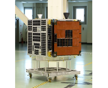
Fig. 3: RAPid Innovative payload demonstration Satelite-1 (RAPIS-1)
 ©JAXA
©JAXA
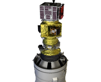
Fig. 4: Innovative Satellite Technology Demonstration-1 (mounting on Epsilon-4)
3. Future development
In the future, NEC will verify the results obtained in this demonstration and promote early operationalization, aiming for further improvement of the performance of NB-FPGA. In addition to artificial satellite equipment, NEC will proceed with expansion into the fields of vehicles and medical devices, where high reliability is required, and contribute to the sophistication of IoT equipment, energy saving and the development of the IoT equipment industry.
***
Notes:
- *1)FPGA
Field Programmable Gate Array. Logic LSI design technology for rewritable field programmable gate arrays. The current market size is 600 billion yen, which is expected to grow in the future.
NanoBridge-FPGA (NB-FPGA)
FPGA using NanoBridge technology enable a tenfold improvement over the power efficiency of conventional FPGAs as well as providing them with high radiation tolerance.
Major specifications
- Logic capacity: Equivalent to 100 K—ASIC gate
- Internal operating voltage: 1.1V; input and output voltage: 1.8 V; maximum inner clock: 256MHz
- Built-in circuit function: Block RAM, PLL
- Package: QFP, BGA
- *2)Project
Project name: Program for Strategic Innovative Energy Saving Technology/Development of 1,000,000 LUT-scale atomic switch FPGA
Period: FY2016 to FY2018
About NEC Corporation
NEC Corporation is a leader in the integration of IT and network technologies that benefit businesses and people around the world. The NEC Group globally provides "Solutions for Society" that promote the safety, security efficiency and fairness of society. Under the company's corporate message of "Orchestrating a brighter world," NEC aims to help solve a wide range of challenging issues and to create new social value for the changing world of tomorrow. For more information, visit NEC at https://www.nec.com.
![]()
LinkedIn: https://www.linkedin.com/company/nec/
YouTube: https://www.youtube.com/user/NECglobalOfficial
Facebook: https://www.facebook.com/nec.global/
Twitter: https://twitter.com/NEC_corp
NEC is a registered trademark of NEC Corporation. All Rights Reserved. Other product or service marks mentioned herein are the trademarks of their respective owners. © NEC Corporation.