
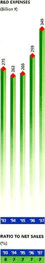
| Research and Development | |
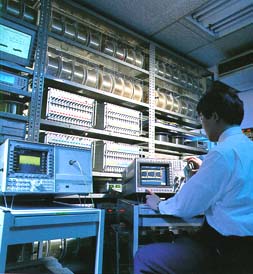
| In the fast-moving electronics market, R&D capability is the key to global competitiveness. NEC focuses its R&D activities on developing leading-edge technologies that advance its existing multimedia businesses and on creating revolutionary technological breakthroughs that contribute to the foundation of new businesses, working to quickly apply the achievements of R&D activities to business operations. With its R&D facilities in Japan, the United States, and Europe working together through the effective sharing of knowledge, NEC is leveraging its global reach to raise its competence. |
 During fiscal 1997, NEC concentrated its R&D activities on high-speed backbone and optical/radio access networks, high-performance computing, natural user interfaces, multimedia filing systems, gigabit-level ultralarge-
scale integrated circuits (ULSIs), highspeed optical devices, nano-scale technologies, and environmental solution technologies.
During fiscal 1997, NEC concentrated its R&D activities on high-speed backbone and optical/radio access networks, high-performance computing, natural user interfaces, multimedia filing systems, gigabit-level ultralarge-
scale integrated circuits (ULSIs), highspeed optical devices, nano-scale technologies, and environmental solution technologies.
In software engineering, NEC actively pursued the advancement of technologies in multimedia network service, groupware work flow, network security, Internet protocol (IP), and higher-value-added microprocessor software. In production engineering, NEC achieved significant advances in core technologies for high-density semiconductor packaging, mechatronics (a combination of mechanics and electronics) applications and production information systems, and such
production-innovation programs as lean production.
During fiscal 1997, NEC started the construction of a new domestic R&D facility in the Kansai area devoted to research in multimedia applications and natural user interface technologies.
NEC successfully performed a basic experiment of optical transmission for 120 kilometers at a world record volume of 2.6 terabits per second (1 terabit=1 trillion bits). A 2.6 terabit per second of information is equivalent to that of 40 million telephone lines. This was achieved using wavelength multiplexing technologies that allow multiple signals of different wavelengths to be transmitted simultaneously through a single optical fiber. NEC views this as a core technology that can enable the super-high-volume data transmission required for new multimedia services in the next century.
With the increasingly widespread use of cellular phones and the miniaturization of PCs and portable information terminals, demand for multimedia information communications using such electronic equipment is growing. NEC has developed the world's first technology that creates a 25Mbps high-speed wireless LAN using a PCMCIA (Personal Computer Memory Card Interface Association) card. Designed to enable high- performance mobile computing, this technology achieves access to such networks as the Internet at speeds up to 12.5 times faster than the wireless LAN systems currently on the market, fast enough to handle high-quality moving picture transmissions.
In joint experiments with the University of Tokyo, NEC has achieved holography through the use of atomic beams, making it the world's first company to do so. Atomic-beam holography relies on a principle of holography in which interference among propagating waves creates three-dimensional images and substitutes streams of atoms for light waves to create an ultrafine pattern surface. This technology represents a significant step forward in atomic-beam lithography to manufacture future ULSIs.
During the period under review, NEC developed a recycling system for PWBs, which are commonly used components in electronic products. This system incorporates special separating and recovering technologies that allow for the low-cost extraction of valuable materials from PWBs. In addition to separating and recovering mounting components and solder by heating and adding forces, the resin board is pulverized and separated based on differences in specific gravity and electrical conductivity. Besides reclaiming such valuable metals as copper and solder, the composite powder of glass fiber and resins can be recovered and used in construction materials.
Beyond simply
salvaging mounting devices, this PWB recycling
system enables the reclamation of the entire PWB, thus eliminating waste.
Internet firewall systems are gaining momentum around the world to more effectively manage and control Internet usage. In fiscal 1997, NEC's SOCKS Internet firewall technology was approved
as one of the Internet standard security protocols by the Internet Engineering Task Force (IETF). In addition, NEC released its latest versions "SOCKS5 and the SOCKS5 Toolkit" which ensure security from infiltration over the Internet through access control.
In contrast to previous firewall systems, which could only verify
Internet protocol (IP) addresses, SOCKS5 can identify individual users regardless of application software. NEC expects this technology to be applied to future mobile computing access control and Internet gateways.
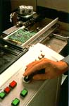
NEC has developed assembly equipment for CSP semiconductors. CSP semiconductors are almost as small as a bare chip, thus playing an important role in designing handheld multimedia equipment. NEC's proprietary Inner Bump Bonding (IBB) production technology allows this CSP to be reduced to the 10-square-millimeter size of a 200-pin-class LSI. To realize a packaging density 10 times higher than that of conventional quad flat packaging (QFP) designs, IBB uses image recognition, precision placement, and high-speed mechanical control technologies for the minute through-hole bonding of LSIs to carrier tape. This new technology is also superior to conventional technology in production efficiency.
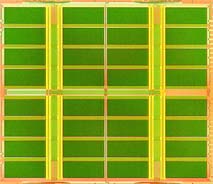
With the development of a 4Mbit cache static random access memory (SRAM) that boasts the world's fastest 500MHz operation, NEC
has improved the level-two cache memory that is essential for enhancing the computing performance of microprocessors. NEC achieved this success by developing a new circuit that enables high-speed operation based on 0.25-micron CMOS processing technology.