The basic objectives of NEC's R&D activities are to continuously develop new technologies, apply knowledge gained through research to tangible business opportunities, and devise better methods of preserving the environment. In fiscal 1995, we focused our R&D efforts on technologies for multimedia information networks, optical access networks, multimedia terminal systems, intelligent interfaces, high-resolution image processing, and CMOS ultra-large-scale integrated circuits (ULSIs).
We also made significant progress in software engineering, most notably in CASE tools, Internet-related technologies, and network management technologies. In the area of production technology, we achieved significant advances in production information systems; semiconductor processing, assembly and packaging; plastic materials applications; and inspection technologies.
In Germany, we opened the C&C Research Laboratories, a division of NEC Europe Ltd. The establishment of this research facility, our first in Europe, underscores the ongoing globalization of our R&D operations.
The "Neo-FishLibrary" pictured on the front cover of this annual report is one example of the type of applications that NEC is developing using hypermedia database technology. In a hypermedia structure, links between multimedia data objects enable users to jump interactively from one object to another. The database features a "drag and drop" interface that facilitates the association of objects, allowing them to be accessed intuitively and quickly. In the future, NEC plans to use this system to create a wide variety of applications, such as electronic museums, video-on-demand, and digital libraries.
In joint experiments, NEC and Japan's Keio University have successfully transmitted data over plastic optical fibers at the breakthrough speed of 2.5Gbits per second. Plastic optical fiber is an attractive transmission medium because it is less expensive and more manageable than glass fiber. However, until now, transmission speeds achieved using plastic fibers were slower than those possible with conventional copper cables. The breakthrough in speed was achieved using high-speed graded index profile plastic optical fibers developed at Keio University and an NEC-made visible light semiconductor laser diode, which served as the transmission light source. NEC developed the light source by modifying a red light semiconductor laser originally designed for use in CD-ROM drives, producing a light source that retained the original device's reliability while providing a tenfold increase in speed over previous plastic fiber transmissions.
In visual programming, a developer's work consists largely of using diagrams displayed on a computer screen to position and create linear connections among icons representing individual program functions. NEC's HOLON/VP is a practical, general-use visual programming tool that enables users with no programming knowledge to develop business applications easily. With HOLON/VP, applications can be developed in a Windows environment with virtually no text-based programming. The tool not only improves development productivity but also simplifies application maintenance.
Semiconductor laser diodes are key components of fiber-optic transmission equipment, CD-ROM drives, and other multimedia-related devices. To verify the quality of these components, the intensify of the light emitted by the diodes must be measured to confirm that its relationship with the electric charge applied to the diode can be described by a smooth, waveform graph. Until now, such inspections required visual confirmation of the waveform pattern by experts. NEC has greatly simplified this process by developing a waveform recognition algorithm that can be used to perform automatic inspections.
NEC places great importance on evaluating the environmental impact of its products and services. Such analysis can be conducted through Life Cycle Assessment (LCA), a quantitative method of determining the burden a product places on the environment over its life cycle, which encompasses manufacture, use, and disposal. In cooperation with Japan's Association of Industrial and Environmental Management and Research Institute for Resources and Environmental Technology, NEC has developed LCA software that quantifies the environmental impact of PCs and other complex electronic devices. The program incorporates a three-dimensional computer-aided design (CAD) system and a database. After analyzing detailed product designs, the software simulates assembly and disposal and generates reports that evaluate the results.
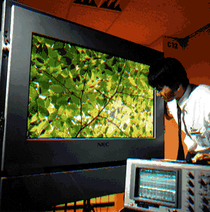
NEC developed this 40-inch color plasma display panel for use in wall-hanging TVs and large-screen multimedia displays. With 1.21 million pixels, this wide display offers one of the highest resolutions and twice the brightness of similar devices in its class.
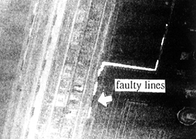
Rapid diagnosis of LSI faults using video images